Day 3: The DGX Spark Unpacked. GB10, Unified Memory, sm_121, and the One Reason This Hardware Exists
A practical teardown of NVIDIA DGX Spark's GB10 Grace Blackwell Superchip, unified memory, sm_121, NVFP4 tensor cores, memory reporting, and decode limits.

On this page (9)
- What's inside the box
- Unified memory: not the same as Apple Silicon
- A real probe: what deviceQuery says about your Spark
- sm121 vs sm100: the Blackwell that isn't datacenter Blackwell
- NVFP4: the format the Spark was built for
- How to read memory state on a Spark (the right way)
- The 273 GB/s decode envelope (the number you should memorize)
- The full picture in one paragraph
- What's coming next
Day 3 of "7 Days of DGX Spark". A field guide to running serious LLMs on a $4,699 box on your desk.
In Day 2 we followed a single LLM request from prompt to answer and learned that memory bandwidth, not compute, is the bottleneck for decode. Today we open the DGX Spark itself and see why this particular hardware was designed the way it was.
By the end of this post, you'll know:
- What's in the GB10 Grace Blackwell Superchip
- What "unified memory" actually means (it's not what your Mac does)
- Why the Spark's GPU has compute capability 12.1 (sm_121), and why that is NOT the same as the 10.0 (sm_100) inside an NVIDIA B200
- What NVFP4 native tensor cores buy you
- How to read memory state on a Spark (and why
nvidia-smilies)
This is also the post that explains why the Spark feels different from every other consumer GPU you've used. The differences are real, intentional, and load-bearing for everything that follows.
Day 1 was the why. Day 2 was the request path. Day 3 is the machine itself.
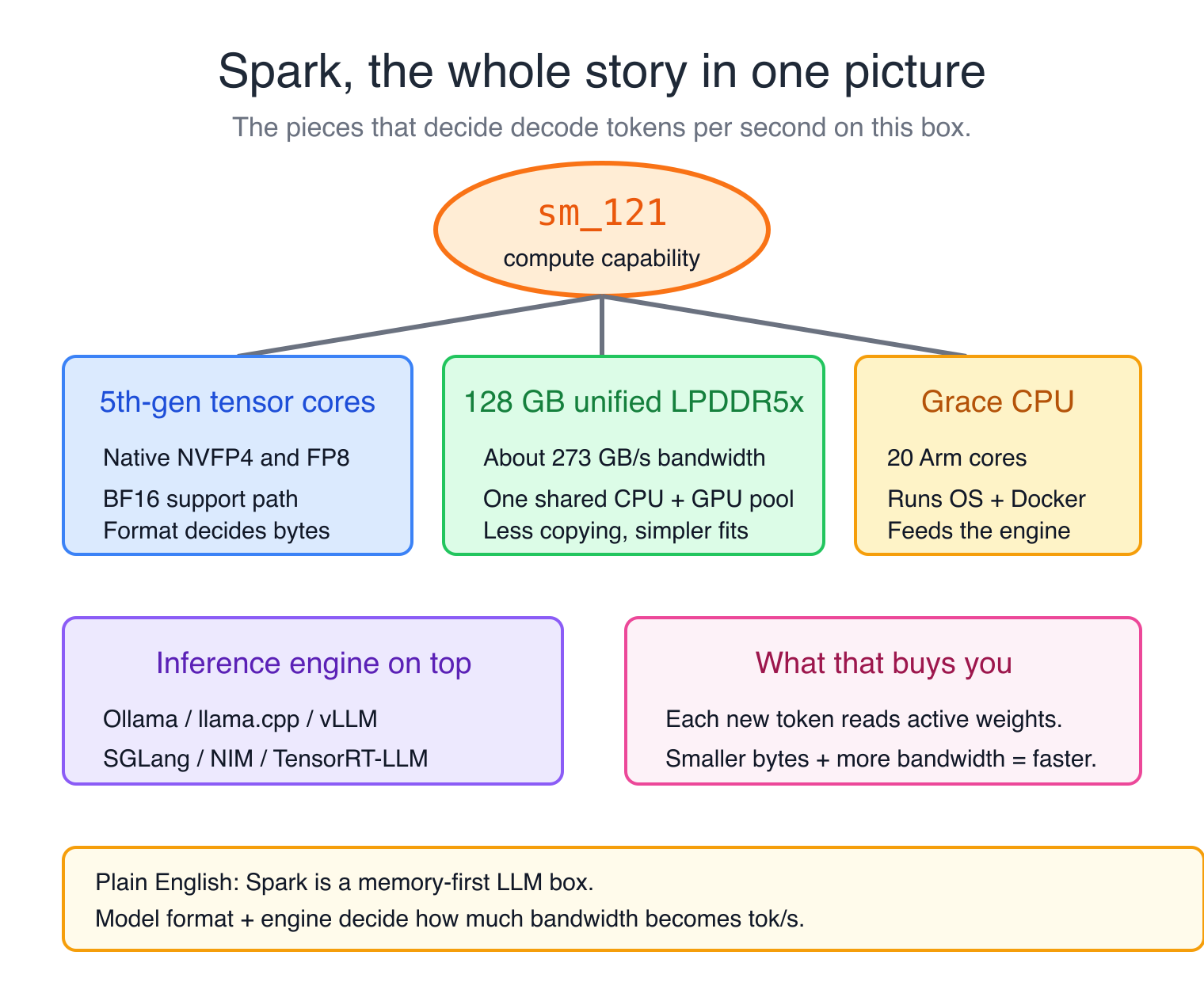
Here's the lens to read this whole post through: once you internalize that decode is memory-bandwidth-bound, the Spark stops looking like a small GPU workstation and starts looking like something more specific, a memory-first LLM box. It is not trying to be a tiny H100. It is trying to give you one big shared memory pool on your desk, plus enough Blackwell tensor-core support to make large models usable. Almost everything below is a consequence of that single design choice.
Animated system view
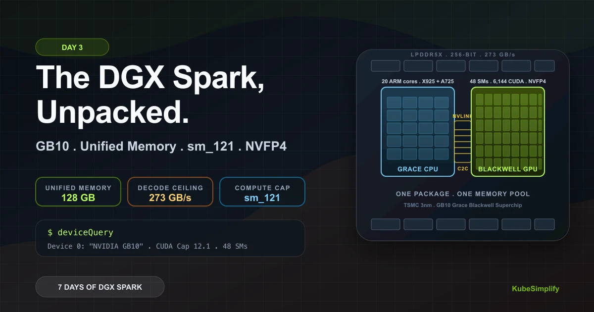
GB10 is two dies feeding one memory pool
The CPU and GPU do not copy model state across a PCIe gap. They share coherent LPDDR5x, which is why capacity is the Spark's real trick.
Grace CPU
20 Arm cores handle tokenization, orchestration, and runtime work.
Blackwell GPU
48 SMs, 6,144 CUDA cores, native FP4 paths, compute capability sm_121.
What's inside the box #
The DGX Spark is small. About the size of a hardback book on its side, 1.2 kg, fits under a monitor. It runs NVIDIA DGX OS 7.5.0, which is Ubuntu 24.04-based. Boots in under a minute. On my unit, the system idles around 4-6 watts and peaks near 150 watts under sustained inference load; NVIDIA's published spec sheet uses a higher system power envelope, and exact numbers depend on workload and ambient temp.
Inside is one main package, not a normal desktop CPU plus a separate add-in GPU. It's called the GB10 Grace Blackwell Superchip, and it's a co-design with MediaTek on TSMC's 3nm process. On that package you get:
- A Grace CPU: 20 ARM cores split as 10 Cortex-X925 (performance) and 10 Cortex-A725 (efficiency), running up to 4.0 GHz. ARMv9.2-A with SVE2, BF16, and i8mm instructions (so the CPU itself is useful for some inference work).
- A Blackwell GPU: 48 Streaming Multiprocessors (SMs), 6,144 CUDA cores total, max clock 2.42 GHz, compute capability 12.1 (we'll come back to this).
- 128 GB of LPDDR5x unified memory: shared between CPU and GPU at ~273 GB/s.
- An NVLink C2C chip-to-chip interconnect between the two dies on the same package.
- External I/O: 10 GbE, Wi-Fi 7, USB-C/HDMI, and ConnectX-7 networking for linking Spark systems.
That's the whole show. One package, two dies, one memory pool.
Small timely aside: on June 1, 2026, NVIDIA and Microsoft announced NVIDIA RTX Spark, a related Grace-plus-Blackwell idea for Windows laptops and compact desktops with up to 128 GB of unified memory. Different product from DGX Spark, but I am excited about that machine too because the NVIDIA + Windows ecosystem coming together could make local agents and local AI workflows feel much more mainstream.
Before we move on, let's decode the spec-sheet words because they show up everywhere:
- TSMC's 3nm process is the manufacturing node used to build the silicon. Smaller nodes usually help with transistor density and power efficiency, but they are not a direct performance number. For us, the practical point is that GB10 can pack a Grace CPU, a Blackwell GPU, and the memory fabric into a compact, low-power desktop package.
- Grace CPU is the general-purpose side of the system. It runs the OS, Docker, Python, tokenization, scheduling, networking, storage, and any CPU-side parts of inference. The GPU does the heavy matrix math; the CPU keeps the whole machine moving.
- ARM cores are CPU cores based on the Arm architecture, not x86 like most Intel/AMD desktops. The practical difference for beginners: some software may need Arm-compatible builds, but modern Linux containers and NVIDIA's stack cover the core AI workflow well.
- Cortex-X925 and Cortex-A725 are two kinds of Arm CPU cores. The X925 cores are the fast cores for heavier work. The A725 cores are efficiency cores for lighter/background work. Splitting them helps the system stay responsive without burning max power all the time.
- Up to 4.0 GHz is the peak CPU clock. It is useful for bursty CPU tasks like preprocessing, installing packages, or moving data around, but LLM generation still mostly depends on GPU memory bandwidth.
- ARMv9.2-A with SVE2, BF16, and i8mm means the CPU supports modern vector and low-precision math instructions. You do not need to memorize the acronyms. In plain English: if some AI/math work falls back to the CPU, the CPU has instructions that make that work less terrible.
- Streaming Multiprocessors (SMs) are the GPU's main work blocks. Each SM schedules groups of threads and contains CUDA cores, tensor cores, registers, cache, and shared memory. When
deviceQuerysays 48 SMs, it means the GPU has 48 of these parallel work islands. - CUDA cores are the scalar execution lanes inside those SMs. They are useful for general CUDA math, but most LLM matrix math runs on tensor cores, not plain CUDA cores. So 6,144 CUDA cores is useful context, not the whole AI-performance story.
- Max clock 2.42 GHz is the peak GPU core frequency. It tells you how fast the GPU can tick under boost, but LLM decode usually waits on memory bandwidth, not clock speed. A higher clock helps only when the workload is compute-bound.
- Compute capability 12.1 is the CUDA architecture target, written as
sm_121. Compilers and libraries use this number to decide which GPU instructions and kernels they can load. - LPDDR5x is low-power DDR memory, the same memory family used in high-end laptops and mobile SoCs. On Spark it is wired as a 256-bit, coherent unified memory pool: slower than HBM, but big, efficient, and shared by CPU and GPU.
- NVLink C2C is the chip-to-chip link between the Grace CPU die and the Blackwell GPU die. It is not the same thing as multi-GPU NVLink between separate accelerators. Here its job is to make the two dies behave like one coherent system.
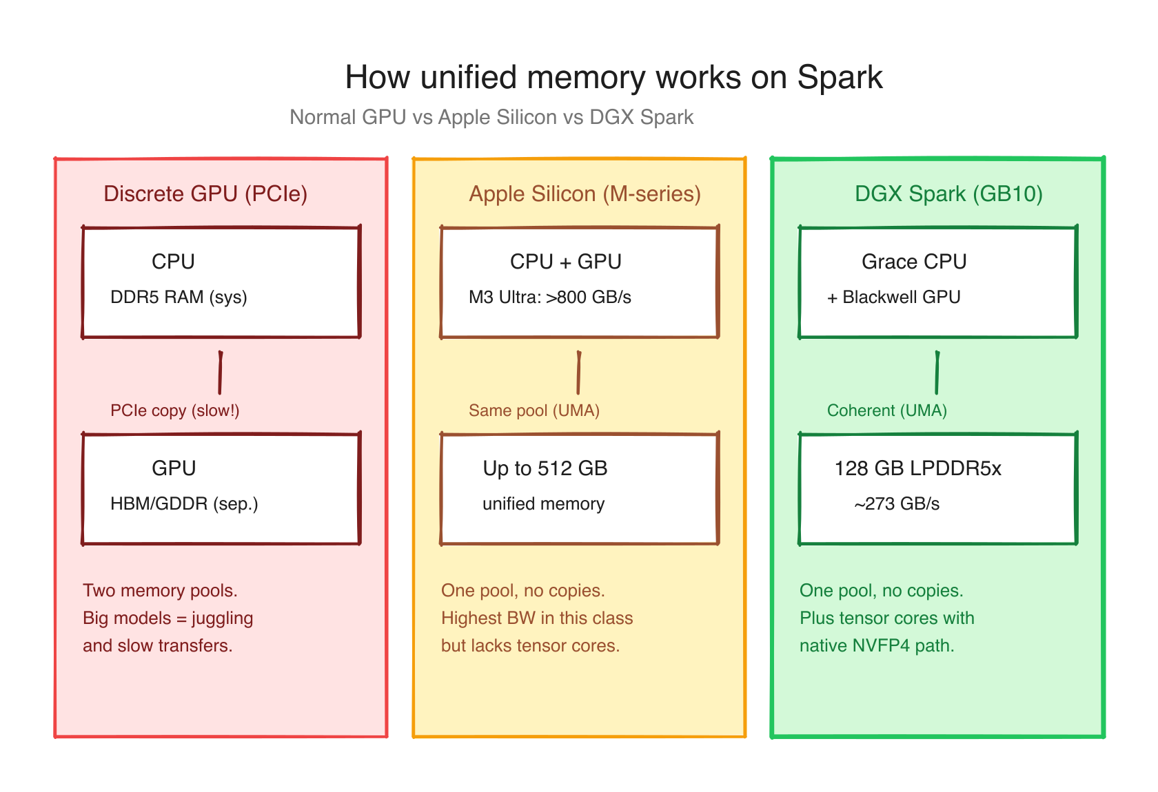
Unified memory: not the same as Apple Silicon #
Both Apple Silicon and the GB10 advertise "unified memory." Both share memory between CPU and GPU. They are NOT the same architecture, and the differences matter.
Apple Silicon (M-series): CPU and GPU sit on the same die and access the same memory pool through a unified memory controller. Bandwidth is high (~800 GB/s on M3 Ultra), capacity is huge (up to 512 GB on Mac Studio). Address spaces are coherent.
This is why Apple's MLX framework exists: it is built for Apple Silicon's shared-memory model instead of treating the GPU like a separate VRAM device. If you want the Mac side of this story, I wrote a full deep dive here: mlxcel: A Rust-Native Inference Engine for Apple Silicon.
NVIDIA GB10 (Spark): CPU and GPU are on separate dies on the same package. They share memory via Address Translation Services (ATS): a hardware feature that maps GPU and CPU virtual addresses to the same physical pages. The bandwidth is ~273 GB/s. Capacity is 128 GB. Address spaces are coherent.
Same idea, slightly different implementations. The practical implication: on a Spark, when you allocate memory from CPU code, the GPU can read it without any cudaMemcpy call. This is enormous for inference engines that used to spend significant time shuffling tensors between host and device.
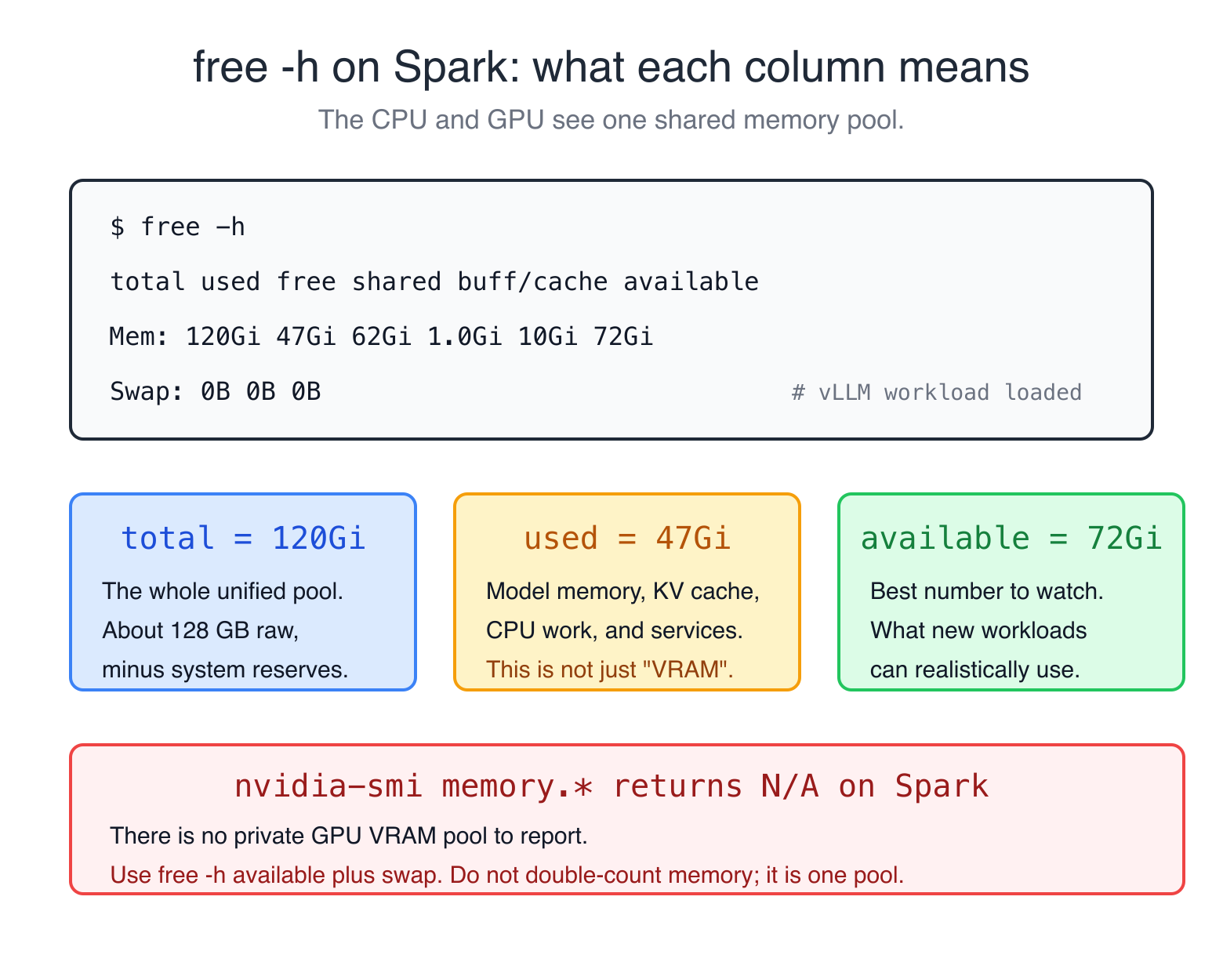
The slightly painful flip side: there's no separate "GPU memory" you can query. Tools like nvidia-smi --query-gpu=memory.used literally return [N/A] on a Spark. There is no "GPU memory used" because there's no separate GPU memory. The pool is one.
Here's the practical rule for Spark's unified memory. The short version: stop reading nvidia-smi for memory state on Spark. Read free -h available instead.
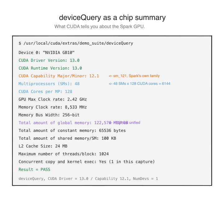
A real probe: what deviceQuery says about your Spark #
If you run NVIDIA's official deviceQuery sample (the diagnostic tool from the CUDA samples) inside a CUDA 13 container on a Spark, you get a very useful hardware snapshot.
One way to reproduce it:
docker run --rm --gpus all nvidia/cuda:13.0.0-devel-ubuntu24.04 bash -lc '
  apt-get update >/dev/null &&
  apt-get install -y --no-install-recommends git make g++ >/dev/null &&
  git clone --depth 1 https://github.com/NVIDIA/cuda-samples /tmp/cuda-samples >/dev/null &&
  make -C /tmp/cuda-samples/Samples/1_Utilities/deviceQuery -j"$(nproc)" >/dev/null &&
  /tmp/cuda-samples/Samples/1_Utilities/deviceQuery/deviceQuery
'
Here's a real output captured from my Spark:
Device 0: "NVIDIA GB10"
  CUDA Driver Version / Runtime Version 13.0 / 13.0
  CUDA Capability Major/Minor version number: 12.1
  Total amount of global memory: 122,570 MBytes
  (048) Multiprocessors, (128) CUDA Cores/MP: 6,144 CUDA Cores
  GPU Max Clock rate: 2,418 MHz (2.42 GHz)
  Memory Clock rate: 8,533 MHz
  Memory Bus Width: 256-bit
  L2 Cache Size: 25,165,824 bytes (24 MB)
  Concurrent copy and kernel execution: Yes with 1 copy engine(s)
  Integrated GPU sharing Host Memory: Yes
  Device supports Managed Memory: Yes
Small caveat: NVIDIA's public hardware overview lists 2 copy engines, while my captured deviceQuery output reported 1 copy engine. I would not build a performance argument on that field until re-checking a fresh sample/driver combination.
Three numbers in there matter most.
122,570 MB total global memory. That's the full 128 GB pool, minus reserved firmware regions. About 119 GiB usable in practice (some of it goes to the OS, some to firmware).
256-bit memory bus × 8,533 MT/s effective memory rate ≈ 273 GB/s. This is the most important number on the chip. It's your decode ceiling for any single model.
Compute capability 12.1. This is the number that explains every weird software bug you'll hit. We talk about it next.
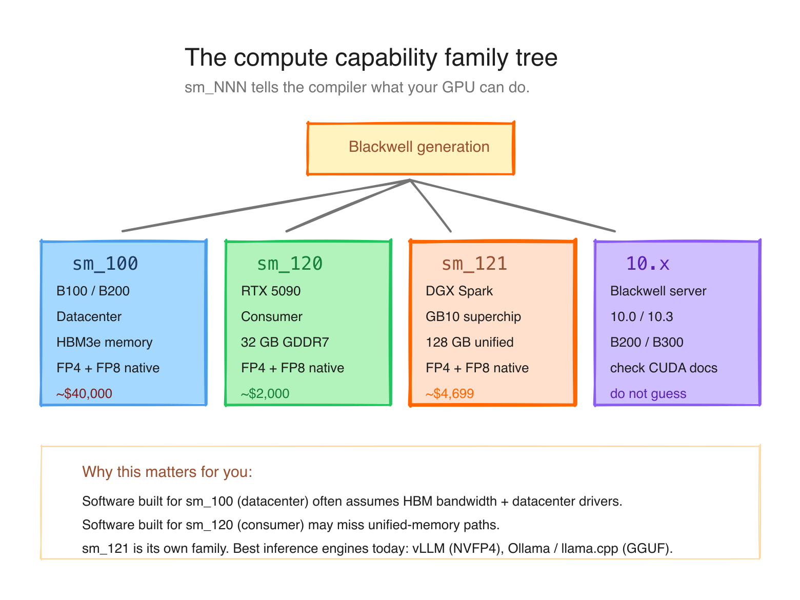
sm_121 vs sm_100: the Blackwell that isn't datacenter Blackwell #
This is the section every reviewer skips and every Spark owner eventually learns the hard way.
NVIDIA's "compute capability" is a version number that identifies what your GPU's instruction set looks like. Every GPU has one. Code is compiled for specific compute capabilities, which is why prebuilt PyTorch wheels sometimes "don't work" on new hardware.
Here's the relevant slice of the family tree:
| Compute capability | Architecture | Class | Examples |
|---|---|---|---|
sm_80 | Ampere | datacenter | A100 |
sm_86 | Ampere | consumer | RTX 3090, A40 |
sm_89 | Ada Lovelace | consumer | RTX 4090, L40 |
sm_90 | Hopper | datacenter | H100, H200 |
sm_100 | Blackwell | datacenter | B100, B200, GB200 |
sm_120 | Blackwell | consumer | RTX 5090, RTX 5080 |
sm_121 | Blackwell | consumer/workstation | GB10 (your Spark) |
What you should notice: Blackwell is not one CUDA target. NVIDIA's current compute-capability table splits Blackwell-era parts across different major/minor targets, including sm_100 for B200/GB200, sm_120 for RTX Blackwell cards, and sm_121 for GB10. The practical point for Spark owners is simple: software built only for datacenter Blackwell (sm_100) is not automatically a native match for GB10 (sm_121).
A kernel compiled only for sm_100 can use code paths that are not valid for sm_121. It won't crash gracefully. It often just refuses to load. If you've ever pulled a prebuilt vLLM image that worked on a B200 and watched it die on your Spark, this is why.
The split also means: many libraries ship prebuilt cubins for sm_80, sm_86, sm_89, sm_90, sm_120 and stop. sm_121 is the youngest member of the family and frequently the last to get explicit support. Workarounds exist (PTX forward compat from sm_120, source rebuilds, community Docker images), and we'll cover them later in the series.
NVFP4: the format the Spark was built for #
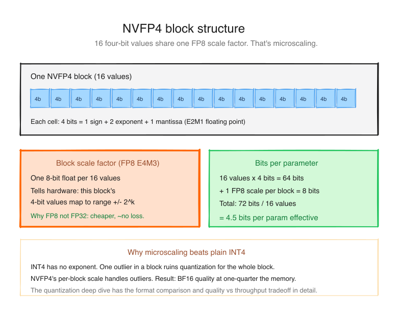
The most important thing the Blackwell tensor cores added is native execution of a 4-bit floating-point format called NVFP4.
A normal FP32 number is 32 bits: 1 sign + 8 exponent + 23 mantissa. FP16 is 16. FP8 is 8. NVFP4 is 4 bits per number. That's tiny: you only get about 16 distinct values per weight.
Naively that would destroy model quality. The trick: microscaling. NVFP4 groups every 16 weights into a "block" and stores a high-precision FP8 scale factor for the whole block. The 4 bits encode the position within the block's range; the shared scale factor tells you what range that is.
Animated quantization view
NVFP4 compresses weights in tiny local blocks
Sixteen 4-bit values share one FP8 scale. That local scale is the reason FP4 can be small without behaving like a blunt integer quant.
Bytes moved per parameter
One NVFP4 micro-block
Compare the three current 4-bit formats:
| Format | Block size | Per-block scale | Notes |
|---|---|---|---|
| INT4 (AutoRound, GPTQ) | 32-128 weights | FP16 scale + INT4 zero-point | Calibrated offline; lossy |
| MXFP4 | 32 weights | E8M0 (8-bit exponent only) | Hardware encoded; coarse |
| NVFP4 | 16 weights | FP8 (E4M3) scale | Hardware encoded; finest |
NVFP4 has the smallest blocks (16 weights) and the highest-fidelity scale (FP8). That means it adapts to local weight variations more finely than the alternatives. In NVIDIA's published material, NVFP4 stays close to FP8 quality on most evals while taking half the bytes per parameter. The next quantization deep dive has the full quality-vs-size breakdown.
Why the Spark cares so much: NVFP4 shrinks a model by nominally 4x vs BF16 (about 3.5x in practice, once you count the per-block scale factors and the layers that stay higher precision). On a 273 GB/s decode-bound machine, cutting bytes-per-parameter that much roughly doubles your decode throughput. NVFP4 is the format that makes a 120-billion parameter Nemotron 3 Super run usefully on a single Spark.
This is where the Nemotron 3 family becomes important. Nemotron 3 is NVIDIA's open model family for agentic workloads: Nano is the smaller efficient tier, Super is the Spark-relevant 120B-A12B MoE tier, and Ultra is the frontier tier. Super is the one we care about on this machine because its NVFP4 artifact is a practical example of why the Spark exists: a model that would be awkward or impossible on normal consumer VRAM becomes a real local workload when the weights are compressed into a large shared memory pool.
And yes, Ultra also belongs in this story. NVIDIA released Nemotron 3 Ultra on June 4, 2026 as a 550B-total / 55B-active MoE model, and NVIDIA's own model page says it was pretrained in NVFP4 and ships a post-trained NVFP4-quantized checkpoint. I would not frame Ultra as "the Spark model" the way Super is; it is much larger and points more naturally at multi-GPU/datacenter Blackwell. But it proves the bigger point: NVFP4 is not just a Spark feature. NVIDIA is building the Nemotron model family and the Blackwell hardware stack around it.
Same model in BF16 = 240 GB and unloadable. Same model in NVFP4 = roughly 60 GB and runs at ~38 tok/s decode NVIDIA published, NVFP4 build via NIM / TensorRT-LLM path. The same architecture as Ollama's Q4_K_M GGUF runs at 19.5 tok/s decode on my Spark [measured 2026-05-21] - different inference engine, different quant, different artifact. Both numbers are correct for what they describe; treat them as different products. The pitch is the same either way: a frontier MoE that wouldn't fit on a 5090, running usefully on a desk machine.
The footnote: NVFP4 wins for inference. Training is a different story (gradients need higher precision in the backward pass), and on Spark today BF16 can actually train faster than NVFP4 at nanochat scale. We cover that paradox in the quantization deep dive.
How to read memory state on a Spark (the right way) #
If you've used a B200 or any other GPU with separate VRAM, your reflex is to nvidia-smi to see GPU memory usage. That reflex is wrong on a Spark.
Try it:
$ nvidia-smi --query-gpu=memory.total,memory.used,memory.free --format=csv
memory.total [MiB], memory.used [MiB], memory.free [MiB]
[N/A], [N/A], [N/A]
Yes. The GPU memory query returns N/A because there is no separate GPU memory. That trips people up constantly, but it is exactly the expected behavior on a unified-memory system: the GPU has no private pool to report.
This was the exact bug I hit in HAMi, and I raised a PR for it. HAMi's NVIDIA device plugin was using NVML's memory API, and on GB10 nvmlDeviceGetMemoryInfo() can return ERROR_NOT_SUPPORTED instead of a normal used/free VRAM result. That bug is fixed now: the plugin can use a preconfigured scheduling budget such as devicePlugin.preConfiguredDeviceMemory: 131072 MiB, register the device, and continue per-pod accounting without panicking. The important lesson is still the same: this does not magically make NVML report live Spark GPU memory. It gives the scheduler a correct budget for a unified-memory device.
So the general Spark rule is:
- Use
deviceQueryfor static GPU facts: name, compute capability, SM count, CUDA cores, clocks, bus width, and total global memory. - Use
free -hfor live memory availability. - Treat NVML/nvidia-smi memory used/free as unsupported on this architecture unless a specific tool documents its own fallback.
Use free -h instead, and read the available column, not free:
$ free -h
               total used free shared buff/cache available
Mem: 120Gi 47Gi 62Gi 1.0Gi 10Gi 72Gi
Swap: 0B 0B 0B
available accounts for the page cache and tells you what you actually have to work with. In this snapshot, 72 GiB is available for new workloads.
The other thing to watch: swap should stay at 0 during inference. If swap starts climbing during a model run, the system is paging weights to disk and your tok/s will crash. Spark's swap is on the same NVMe as everything else, which makes the death spiral worse. The fix is to lower --gpu-memory-utilization or pick a smaller model.
The 273 GB/s decode envelope (the number you should memorize) #
In Day 2 we said decode is memory-bandwidth-bound, and the theoretical maximum decode tok/s is bandwidth / model_size_in_bytes. Today let's put real model sizes against the 273 GB/s number to see the practical envelope on a Spark.
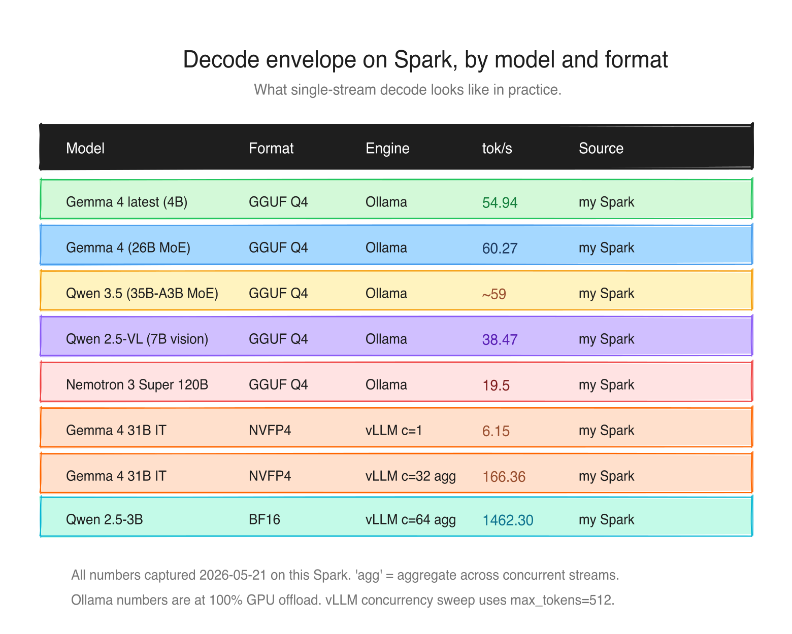
| Model | Resident size | Bytes per token | Theoretical max | Measured | Source |
|---|---|---|---|---|---|
| llama 3.1 8B Q4 | 4.5 GB | 4.5 GB (dense) | ~60 | 38 | Ollama official |
| GPT-OSS 20B MXFP4 | 13 GB | ~3.6 GB (4/32 experts) | ~75 | 58 | Ollama official |
| deepseek-r1 14B Q4 | 8 GB | 8 GB (dense) | ~34 | 20 | Ollama official |
| Gemma 4 26B MoE (Q4_K_M, 8/128 experts) | 15 GB | ~2.2 GB (3.8B active) | ~124 | 65.6 | my Spark, llama.cpp + CUDA |
| Qwen 3.5 35B-A3B (Q4 MoE) | 23 GB | ~1.8 GB (3B active) | ~152 | ~59 | my Spark |
| Llama 3.3 70B NVFP4 | 35 GB | 35 GB (dense) | ~7.8 | not measured here | envelope estimate |
| Nemotron 3 Super 120B-A12B (Q4 GGUF) | 86 GB on disk | ~6 GB (12B active) | ~45 | 19.5 | my Spark, Ollama |
| Nemotron 3 Super 120B-A12B NVFP4 | ~60 GB | ~6 GB (12B active) | ~45 | ~38 | NVIDIA published (NIM / TRT-LLM) |
A couple of things to notice.
The Mixture-of-Experts (MoE) models beat their dense-model bandwidth limits. That's because in an MoE only the active parameters are read per token: Qwen 3.5 35B-A3B has 35B total but only 3B active per token, so the effective decode size is closer to 3B at ~2 GB, giving ~152 tok/s theoretical. The measured ~59 tok/s shows the gap from ideal - KV cache reads, routing overhead, kernel fusion limits. MoE is Spark's superpower. The leaderboard post later in the series unpacks this fully.
The dense 70B in NVFP4 is right at the theoretical floor: single-digit tok/s for a 35 GB read at 273 GB/s. Dense 70B on Spark is genuinely hard and probably not the right tool unless you really need it.
The Nemotron 3 Super row shows the engine/format gap clearly: 19.5 tok/s on Ollama's Q4_K_M GGUF [my measurement] vs ~38 tok/s on NVIDIA's NVFP4 build [NVIDIA published]. Same weights, different artifacts, different kernels. Always check which inference engine + quant a benchmark used before comparing.
The full picture in one paragraph #
The DGX Spark is a single-package design where a Grace ARM CPU and a Blackwell consumer GPU share one 128 GB pool of LPDDR5x memory at 273 GB/s. The GPU is sm_121, which is a different instruction set from datacenter Blackwell's sm_100 and frequently the last variant to get prebuilt library support. The headline hardware feature is native NVFP4 tensor cores, which let frontier-class models compress to a quarter of their BF16 size while keeping near-FP8 quality. The hardware's pitch is not "fast tok/s" (memory bandwidth caps decode at the speed you'd expect from a desktop chip) but rather "a 120-billion parameter model runs at usable speeds on your desk and you can develop against it without renting cloud GPUs."
That's the box.
What's coming next #
In the next post we go deep on quantization. We've used NVFP4 as the running example here, but there is a full menu of precision and quantization choices: BF16, FP8, MXFP4, NVFP4, INT4-style formats, and GGUF formats such as Q4_K_M and IQ3_XXS. The goal is practical: when to use which format, what it costs in quality, what it buys in speed on a Spark, and why BF16 can sometimes be the better choice for small training workloads even though NVFP4 wins the inference story.
See you in the next post.
References for this post: my own captured deviceQuery output on this Spark (2026-05-08), NVIDIA DGX Spark specifications, NVIDIA DGX Spark User Guide, Arm Learning Path for GB10 system readiness, NVIDIA CUDA GPU compute capability table, NVIDIA CUDA Programming Guide: Unified and System Memory, NVIDIA NVFP4 technical blog, NVIDIA Nemotron 3 family, NVIDIA Nemotron 3 Ultra, NVIDIA Nemotron 3 Super technical blog, Ollama: NVIDIA DGX Spark performance, build.nvidia.com/spark/nvfp4-quantization, NVIDIA and Microsoft RTX Spark announcement, Project-HAMi PR #1841.
Saiyam is working as Head of DevRel at vCluster Labs. He is the founder of Kubesimplify, focusing on simplifying cloud-native & AI infrastructure. He is KubeCon Co-chair and has worked on many facets of Kubernetes, including machine learning platforms, scaling, multi-cloud, & managed Kubernetes services. When not coding, Saiyam contributes to the community by writing blogs and organizing local meetups for Kubernetes and CNCF. He is also a CNCF TAG OpsRes Chair & can be reached on Twitter @saiyampathak.
Get new posts in your inbox.
Spotted a typo or want to improve this post? Edit on GitHub →